
Full-feature PCB manufacturing.
Co-engineering, quick-turn prototypes and volume fabrication of multilayer, HDI and specialty boards — to IPC and ISO standards.
End-to-end manufacturing support
Co-Design & Co-Engineering
We work with your engineers to balance cost, manufacturability and performance, using Valor-class DFM/DFA tools before any panel is built.
Quick-Turn Prototyping
Fast prototype builds on the same high-end equipment and process controls used for volume production — so prototypes behave like production.
Volume Fabrication
Stable, repeatable production of multilayer and HDI boards with in-process inspection and full electrical test.
What we fabricate
Our core specialisation is HDI and semiconductor test boards, supported by a full range of board technologies.
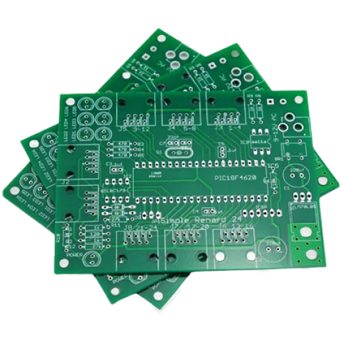
Standard Multilayer
4–20 layer FR4 and High-Tg boards
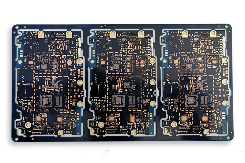
HDI / Any-Layer
Microvias, stacked vias, fine lines
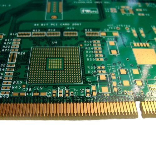
Gold-Finger Boards
Hard-gold edge connectors
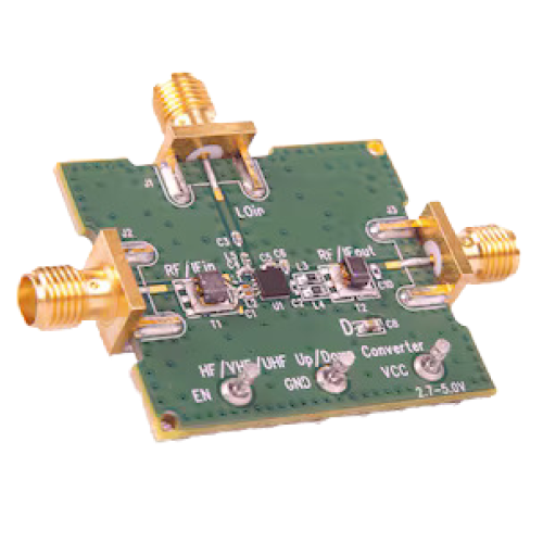
RF & High-Frequency
Low-loss laminates, tight impedance

Metal-Core / Aluminium
Thermal management for power & LED
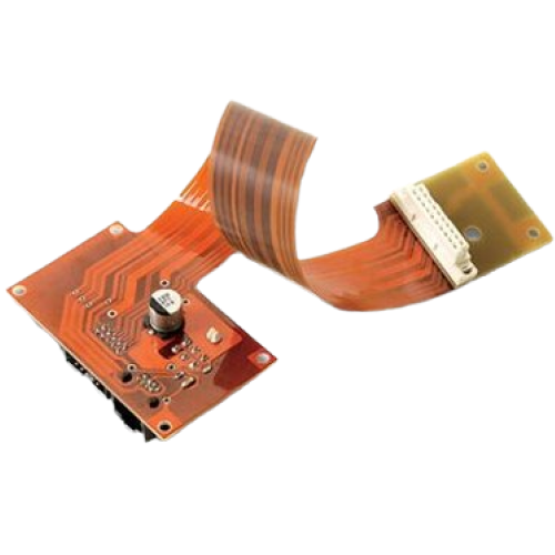
Flex & Rigid-Flex
Polyimide flex for compact assemblies
Fabrication capabilities
Typical capability ranges. Contact us for requirements outside these limits.
| Parameter | Standard | Advanced / HDI |
|---|---|---|
| Layer count | 1 – 20 | Up to 40 |
| Min trace / space | 4 / 4 mil | 3 / 3 mil |
| Min mechanical drill | 0.20 mm | 0.15 mm |
| Min laser microvia | — | 0.10 mm |
| HDI structures | — | 1+N+1, 2+N+2, stacked & staggered, any-layer |
| Board thickness | 0.4 – 3.2 mm | Up to 6.0 mm |
| Copper weight | 0.5 – 3 oz | Up to 6 oz |
| Impedance tolerance | ±10% | ±7% on request |
| Materials | FR4, High-Tg FR4 | Low-loss / high-frequency, polyimide, metal-core |
| Surface finishes | HASL (LF), OSP, ENIG | ENEPIG, immersion silver / tin, hard gold |
| Standards | IPC-A-600 Class 2 | IPC-A-600 Class 3 |
Quality built into every step
Inspection and test are part of the process, not an afterthought at the end of the line.
- Incoming material inspection
- Automated optical inspection (AOI) on inner and outer layers
- Impedance testing with TDR coupons
- Microsection and X-ray analysis for vias and registration
- 100% electrical test — flying probe or fixture
- Final visual inspection to IPC-A-600
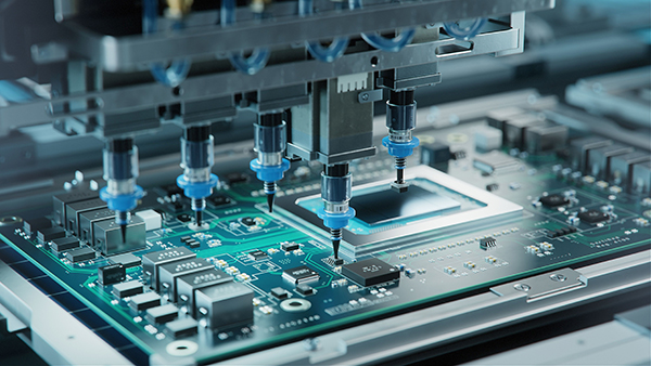
Our fabrication flow
CAM & Imaging
Data preparation, inner-layer imaging and AOI.
Lamination & Drilling
Press, mechanical and laser drilling.
Plating
Copper plating and via fill for HDI.
Outer Layers & Mask
Imaging, etch, solder mask and legend.
Finish & Test
Surface finish, routing and electrical test.
Have a board in mind? Let’s talk.
Send us your Gerbers, BOM or just an idea. Our engineers will come back with a DFM review and a quotation.